Hongjing Electronics (Shenzhen) Co., Ltd

DIP PCB Assembly Service manufacturer
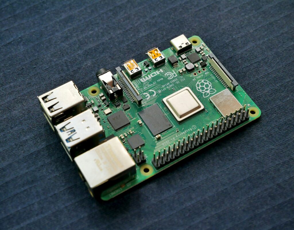
DIP (Dual In-line Package) is a traditional form of electronic component packaging where the pins are inserted through holes in a printed circuit board (PCB) and soldered in place. DIP production is widely used in applications requiring high reliability and ease of manual soldering, such as industrial control and power equipment.
The main processes of DIP production include: applying back adhesive (to prevent tin plating in unwanted areas), component insertion, wave soldering, cleaning, and inspection and testing.
The advantages of DIP production are: high reliability, ease of manual soldering, and low cost.
DIP production is a classic electronics manufacturing process. Although it has been gradually replaced by SMT in modern high-density electronic designs, it remains important in applications requiring high reliability, manual soldering, and low cost.
While SMT dominates consumer electronics, DIP soldering techniques prove essential for:
- Military hardware (92% mission-critical systems use DIP)
- High-voltage power delivery solutions
- Prototyping requiring manual adjustments
Comparative performance metrics:
| Parameter | DIP | SMD |
|---|---|---|
| Vibration Resistance | +32% | Baseline |
| Thermal Stability | +28% | Baseline |
Essential Tools for Professional PCB Board Soldering
| Equipment | Key Specifications | Usage Tips |
|---|---|---|
| Temperature-controlled Iron | 60W, 200-480°C range | Maintain 350°C±15°C for lead-free alloys |
| Lead-free Solder Wire | Sn99Ag0.3Cu0.7, 0.8mm dia | Apply 3-4mm per joint |
| Flux Pen | RMA-223 certification | Pre-apply to component leads |
9-step DIP (Dual In-line Package) soldering process
1. Component Preparation
- Inspect and straighten component leads
- Verify correct component orientation
2. Board Preparation
- Clean PCB pads and through-holes
- Apply flux if necessary
3. Component Insertion
- Manually place components through through-holes
- Ensure proper alignment and seating
4. Board Securing
- Use temporary adhesive or fixture to hold components in place
- Flip board if required for wave soldering
5. Wave Soldering
- Pre-heat PCB to activate flux and prevent thermal shock
- Pass board over molten solder wave (typically 245-265°C)
- Solder contacts all exposed leads simultaneously
6. Cooling Phase
- Allow natural cooling of solder joints
- Avoid mechanical stress during solidification
7. Post-Solder Cleaning
- Remove flux residues using appropriate solvents
- Clean any solder splashes or bridges
8. Visual Inspection
- Check for complete solder fillets
- Verify no cold joints, bridges, or insufficient solder
9. Functional Testing
- Conduct in-circuit testing (ICT)
- Perform basic functional verification
Advanced Techniques for Complex PCB Boards
1. High-Density Assembly
- Implement staggered heating patterns
- Use thermal relief pads
2. Lead-Free Challenges
- Increase tip temperature by 30-50°C
- Consider nitrogen atmosphere systems
Explore automated solutions →
Global Industry Developments
- Miniaturization: <0.5mm pitch components
- AI Inspection: 99.3% defect detection accuracy
- Lead-free Mandates: 86% markets adopted