Hongjing Electronics (Shenzhen) Co., Ltd

PCB Service manufacturer
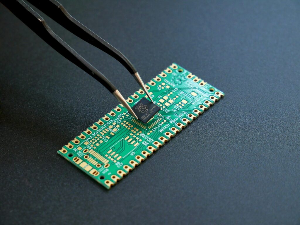
PCB (Printed Circuit Board) is a substrate made of insulating materials (such as FR-4), with conductive copper layers formed on its surface through printing or etching processes to create circuit patterns. Electronic components are fixed onto the PCB by soldering and connected electrically through copper traces.
From consumer electronics (smartphones, smart home devices) and automotive electronics (ECUs, sensors) to medical equipment (patient monitors, wearables), industrial control systems (PLCs, robots), and communication devices (5G base stations, routers), one technology silently powers the functionality of modern electronics – the Printed Circuit Board (PCB).
As the “skeleton” and “neural network” of electronic devices, the PCB industry directly influences the pulse of global technological advancement. Serving as the fundamental carrier for electrical connections between components, PCBs have evolved from simple single-layer boards to today’s high-density interconnect (HDI) and flexible circuits, driving continuous innovation across industries.
With the rise of 5G, IoT, and AI technologies, PCB manufacturing is embracing new challenges in miniaturization, high-frequency performance, and thermal management. The industry’s development trajectory mirrors the technological transformation of our era, making it a critical enabler of the digital revolution.
I. PCB: The Infrastructure of the Digital World
PCBs interconnect electronic components through copper traces on insulating substrates, with their design and manufacturing quality defining the performance limits of end products. Ranging from simple single-layer boards to complex 20-layer high-density interconnects (HDIs), PCBs are ubiquitous in:
- Consumer Electronics (smartphones, laptops)
- Telecommunications (5G base stations, routers)
- Automotive Electronics (ADAS, battery management systems)
- Industrial & Medical Systems (robotics, imaging devices)
- Aerospace (satellites, navigation systems)
According to Prismark, the global PCB market surpassed $80 billion in 2023, with China accounting for over 50% of production, cementing its role as the industry’s manufacturing hub.
II. Innovation: Fueling the Next Wave of PCB Evolution
To meet demands for smaller, faster, and more powerful electronics, the industry is advancing through four key technological frontiers:
- High-Density Interconnect (HDI) and Substrate-Like PCBs (SLP)
- HDI enables multilayer precision routing via microvias and ultra-fine traces, becoming critical for 5G smartphones and wearables. Apple’s iPhones now use SLPs with trace widths/spacing below 30μm.
- Flexible PCBs (FPCs) and Rigid-Flex Solutions
- Foldable devices (e.g., Samsung Galaxy Fold) and automotive sensors rely on FPCs’ bendable properties, driving explosive demand.
- Material Breakthroughs
- High-frequency laminates (e.g., Rogers’ PTFE) support 5G mmWave applications.
- Ceramic and metal-core PCBs address thermal challenges in high-power LEDs and EVs.
- Smart Manufacturing
- Laser drilling, automated optical inspection (AOI), and AI-driven factories boost yields, with top-tier manufacturers achieving over 80% automation.
III. Growth Opportunities: Three Explosive Markets
- 5G and AIoT Infrastructure
- 5G base stations require 3x more PCBs than 4G, with high-frequency materials.
- Edge computing and AI servers drive demand for advanced, high-layer-count PCBs.
- The Electric Vehicle (EV) Revolution
- EVs demand high-reliability PCBs for battery management, ADAS, and infotainment, increasing PCB value per vehicle by 5x+ compared to traditional cars.
- Localization and Supply Chain Reshaping
- Companies like Huawei and Xiaomi prioritize domestic PCB suppliers. Chinese leaders like Shennan Circuits and Wus Circuit now compete globally in high-end markets.
IV. Challenges and Trends: Sustainability and Convergence
Despite growth, the industry faces hurdles:
- Environmental Compliance: Stricter regulations on etching wastewater, copper recovery, and halogen-free materials.
- Cost vs. Performance: Reliance on imported high-end materials (e.g., IC substrates) remains a bottleneck.
- Convergence with Semiconductors: Blurring lines between PCB fabrication and advanced packaging (e.g., SiP, chiplets).
Future trends will focus on:
- Green Manufacturing: Zero-discharge wastewater systems and biodegradable substrates.
- Integration and Modularization: PCBs evolving into multifunctional modules, merging with semiconductor packaging.
V. Conclusion: The Silent Engine of Innovation
Though rarely in the spotlight, PCBs are indispensable to the digital age. As AI, 6G, and quantum computing emerge, PCB innovation will continue to break boundaries. For Chinese manufacturers, mastering high-value segments—like IC substrates and advanced materials—will determine their leadership in the next decade.
Those who unlock the DNA of PCB evolution will dominate the next era of electronics.
Sources: Prismark, CPCA, Corporate Filings
Food for Thought:
- As PCB trace widths approach physical limits, will 3D stacking redefine the industry?
- Can bio-based PCB materials transition from labs to mass production under net-zero goals?
Share your insights in the comments!