Hongjing Electronics (Shenzhen) Co., Ltd


Custom 4-Layer PCB Manufacturer | FR4 1.6mm Board | 1oZ Copper Thickness | ENIG Surface Finish | Green Solder Mask & White Silkscreen
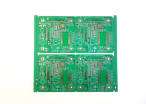
Green Printed Circuit Board ENIG 8 Layer shenzhen printed circuit board manufacturers PCB Manufacturing
Brand Name: HJ-PCBA
Model Number: HJ-PCBA-30289
MOQ: 1 pc
Payment Terms: Paypal / , T/T
Supply Ability: 15000-25000square meters per month
Custom 4-Layer PCB Manufacturer | FR4 1.6mm Board | 1oZ Copper Thickness | ENIG Surface Finish | Green Solder Mask & White Silkscreen
1.Detailed Specifications
| Material | FR4 |
| Board Thickness | 1.6mm |
| Surface Treatment | ENIG |
| Copper Thickness | 1/1 OZ |
| Soldermask | Green |
| Silkscreen | White |
| The Min Laser Drill Hole | 6 Mill |
| Panel | Breakaway |
2.More pictures
3.Manufacturing Capacity – Rigid PCB
| Item | Production Capacity |
| Product Type | Single/Double/Multilayer (1-20 Layers) |
| Material Thickness | 0.4-4.0mm (±10% tolerance) |
| Max BoardSize | Single/Double:600x1500mm |
| Multilayer:600x1200mm | |
| Material | FR-4(TG130-180),Aluminum, Polyimide.etc. |
| CopperWeight | 18-300um (1/20Z-80Z) |
| Min L/S | Inner 75um/Outer 50um |
| Surface Finish | Lead-free HASL, ENlG, lmmersion Silver,OSP |
| Edge Connector | Hard Gold Plating: Ni5um+Au0.25-0.5um |
| Driling | Mechanical:0.15-6.5mm |
| Laser: 0.1-0.15mm(Micro-vias) | |
| lmpedance | +8%(Standard) |
| +5%(Prequalification required) | |
| Continuity Test | 500V DC/12.000 Test Points |
| Solderability | Leaded:235-C/20s |
| Lead-free:260°C/30s | |
| V-CUT | Depth Tolerance +0.1mm |
| Min PanelSize 50x50mm |
Introduction:
The PCB (Printed Circuit Board) is an indispensable core component in electronic devices, used to connect and support electronic components, enabling electrical connections and signal transmission in circuits.
PCB Production:
PCB (Printed Circuit Board) is a substrate made of insulating materials (such as FR-4), with conductive copper layers formed on its surface through printing or etching processes to create circuit patterns. Electronic components are fixed onto the PCB by soldering and connected electrically through copper traces.
The main components of a PCB include:
– Substrate (typically made of insulating materials, providing mechanical support and electrical insulation).
-Copper Layer (conductive circuits formed on the substrate through etching processes, used for transmitting electrical signals).
– Pad (metal areas used for soldering electronic components).
– Via (used to connect circuits between different layers, classified as through-hole, blind via, and buried via).
– Solder Mask (a protective layer covering the copper layer to prevent short circuits and oxidation, usually in colors such as green, blue, white, black, or red).
– Silkscreen (text or symbols printed on the PCB surface to identify component locations, part numbers, and other information).
Factory Introduction:
Hongjing Electronics (Shenzhen) Co., Ltd., as a professional PCB and PCBA custom manufacturer, provides customers with high-precision, high-reliability** circuit board manufacturing and assembly services. Below are the company’s key advantages and service offerings:
1. PCB Manufacturing Capabilities
– Product Types:
– Single-sided, Double-sided, Multilayer Boards (4-32 layers)
– HDI Boards (High-Density Interconnect)
– High-Frequency Boards (for RF and microwave communication)
– Metal Core Boards (Aluminum/Copper Base) (for LED lighting, power modules)
– Gold Finger Boards (high wear resistance, for connectors)
– Blind/Buried Via Boards (high-complexity PCBs)
– Material Options:
– FR-4, High-Tg materials, High-frequency materials (Rogers, Teflon), Aluminum substrates, etc.
– Process Capabilities:
– Minimum trace width/spacing: 3mil (0.075mm)
– Minimum hole size: 0.15mm (laser drilling)
– Surface finishes: ENIG, Immersion Silver, OSP, HASL, Electroplated Gold, etc.
2. PCBA Assembly Services (SMT/DIP)
– SMT Assembly (high-speed, high-precision placement)
– DIP Assembly (through-hole component soldering)
– BGA, QFN, LGA Package Soldering
– Testing & Inspection (AOI, X-ray, functional testing)
3. Target Industries
– Industrial Control (PLC, industrial motherboards)
– Communication Equipment (5G base stations, RF modules)
– Security & Surveillance (camera PCBs)
– LED Lighting (thermal management solutions)
– Consumer Electronics (smart home, wearables)
– Medical Electronics (high-reliability PCBs)
4. Customized Services
– Production based on Gerber files, with DFM optimization
– Small & large batch production (flexible lead times)
– Supply Chain Support (component sourcing, BOM matching)
5. Why Choose Hongjing Electronics?
✅ High-Precision Manufacturing (IPC standards compliant)
✅ Strict Quality Control (100% electrical testing & reliability checks)
✅ Fast Response (dedicated technical support)
✅ One-Stop Service (PCB + PCBA full-process solution)
If you have PCB design, prototyping, or mass production needs, feel free to share your Gerber files,BOM lists or technical specifications, and we will provide the optimal solution!
📞 Contact Us:
- Email: [hjpcbassemblysmt@gmail.com]
- Phone: [18929375891]
Looking forward to collaborating with you! 🚀
| Brand Name | HJ-PCBA |
|---|---|
| Model Number | HJ-PCBA-30289 |
| MOQ | 1 pc |
| Payment Terms | Paypal / , T/T |
| Supply Ability | 15000-25000square meters per month |
Related products

ENIG 8 Layer pcb factory pcb assembly PCB Manufacturing shenzhen printed circuit board 1
Get Best PriceENIG 8 Layer pcb factory pcb assembly PCB Manufacturing shenzhen printed circuit board 3
Get Best PriceENIG 8 Layer pcb factory pcb assembly PCB Manufacturing shenzhen printed circuit board 1
Get Best PriceCustom 6-Layer FR4 PCB Manufacturer | 2oZ Copper Thickness | 1.6mm Board | Blue Solder Mask | OSP Surface Finish
Get Best Price


Reviews
There are no reviews yet.