Hongjing Electronics (Shenzhen) Co., Ltd
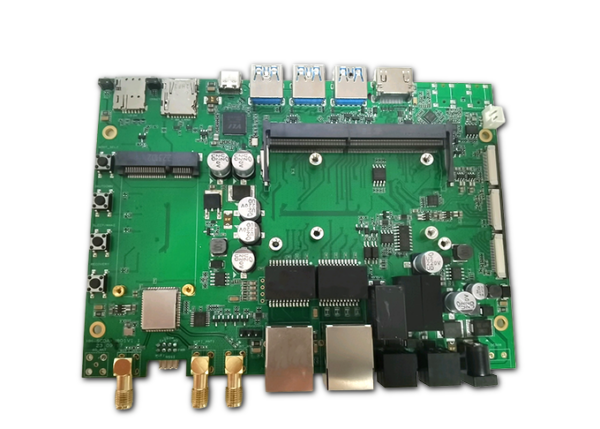
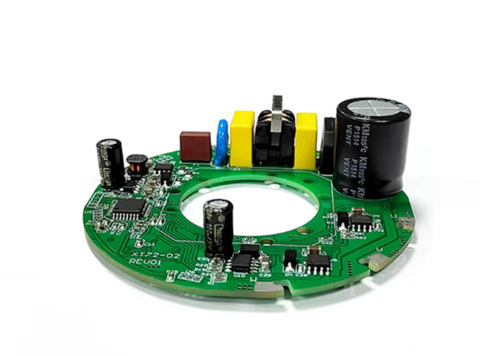
6-Layer PCB Manufacturing | TG170 2.0mm Board | ENIG 2U” RoHS | SMT+DIP PCBA | PCB Assembly | 2oz Copper Thickness
6-Layer PCB Manufacturing | TG170 2.0mm Board | ENIG 2U” RoHS | SMT+DIP PCBA | PCB Assembly | 2oz Copper Thickness
Place of Origin: Shenzhen, China
Brand Name: HJ-PCBA
Model Number: HJ-PCBA-30286
MOQ: 1 pc
Payment Terms: Paypal / , T/T
Supply Ability: 15000-25000square meters per month
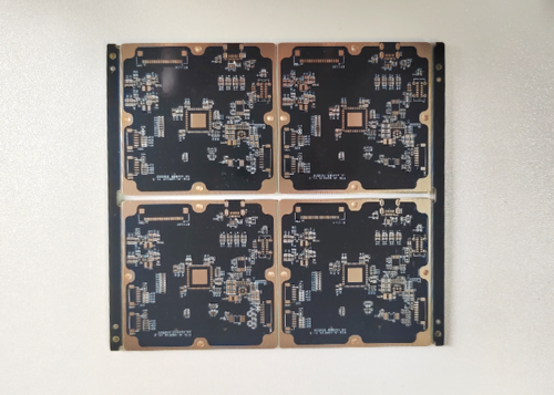
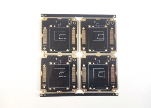
6-Layer PCB Manufacturing | TG170 2.0mm Board | ENIG 2U” RoHS | SMT+DIP PCBA | PCB Assembly | 2oZ Copper Thickness
Detailed Specifications
| Material | TG170 |
| Board Thickness | 2.0mm |
| Surface Treatment | ENIG |
| Copper Thickness | 2/1/1/1/1/2 oz |
| Soldermask | Green |
| Silkscreen | White |
| The Min Laser Drill Hole | 6Mill |
| Panel | Mouse Bite |
Product Description
1.PCB Assembly Services Overview
Product : Multilayer Printed Circuit Board (Multilayer PCB) designed for security equipment applications.
Order Flexibility : Prototype, small, medium, and large-volume production supported. No MOQ required for new orders.
Certifications : Full compliance with UL, IATF 16949 (automotive), RoHS, ISO 9001, and other industry standards.
2.Specification Of PCB Assembly Service
| CATEGORY | PARAMETER | SPECIFICATIONS | TECHNICAL NOTES |
| Substrate | Layers | 1-20 Layers | Complies with IPC-4101 Class 2 standards |
| Material | FR-4,CEM-1/3 ,High Tg (>170°C), Halogen-Free FR4,FR-1/2, Aluminum Core PCB | Thermal Conductivity of Aluminum Core PCB ≥2.0 W/(m·K) | |
| Board Thickness | 0.2mm-7mm | Tolerance: ±10% | |
| Fabrication | Max. Board Size | 500mmx500mm | Supports Panelization |
| Min. Drill Hole Size | 0.25mm | Mechanical Drilling (Minimum drill bit size: 0.25mm) | |
| Min. Line Width/spacing | 0.075mm(3mil) | Supports High Density Interconnect (HDI) | |
| Surface Finish | Surface Finish | HASL(Lead-Free HASL), Chemical Tin, ENIG, lmmAg,OSP, Gold Plating | ENIG (Electroless Nickel Immersion Gold): Nickel thickness 3-5μm, Gold thickness 0.05-0.1μm (per IPC-4552) |
| Solder Mask Color | Green/Black/white/Red/Blue/Yellow | Matte/Gloss Finish available | |
| Copper Thickness | 0.5-4oz (17-140um) | Outer layer copper thickness ≥1 oz (35μm) | |
| Tolerance | PTH Hole Tolerance | ±0.076mm | Complies with IPC-6012 Class 2 |
| NPTH Hole Tolerance | ±0.05mm | ||
| Packing | Inner Packing | Vacuum Sealing + ESD Bag | Moisture Sensitive Devices (MSDs) controlled per MSD Level 3 (IPC/JEDEC J-STD-033) |
| OuterPacking | Standard Carton | ptional anti-shock padding or custom wooden crate | |
| Certifications | Certificates | UL,ISO9001.IS014001. ROHS.CQC | Supports lead-free process (IPC J-STD-001) |
| Profiling | Profiling Method | Routing、V-CUT、Beveling | V-CUT depth controlled to ±0.1 mm (when board thickness is 1.6 mm) |
| Assembly | Assembly Service | ull-range PCBA OEM/ODM Services | SMT placement accuracy ±0.025 mm (Cpk ≥1.33), DIP insertion yield ≥99.95%; Support for ICT/FCT testin |
3.PCB Assembly(SMT) Product Capacity
| CAPABILITY CATEGORY | TECHNICAL SPECIFICATIONS | |
| SMT Capacity | Max. PCB Size: 510mm x1200mm(SMT Process) | |
| Supported Components: 0201.0402.0603.0805.1206 | ||
| Packages | ||
| Min. lC Pin Pitch: 0.1mm | ||
| Min. BGA Pitch: 0.1mm | ||
| IC Placement Accuracy | ||
| +0.01mm(CPK=1.67) | ||
| Daily Capacity: ≥8 MillionPoints/Day (Dual Shifts) | ||
| DIP Capacity | 3 Full-Automatic DlP Lines(Wave Soldering/SelectiveSoldering) | |
| Testing Services | Standard Tests | .Bridgeest .AOl Inspection .X-Ray Analysis .FlyingProbe |
| Functional Tests | .In-CircuitTest (lCT) .Functional Test(FCT) .Thermal Cycling | |
| Reliability Tests | .DropImpact (lEC 60068-2-32) .Burn-In (72H@85°C/85%RH) | |
| Custom Tests | .WaterproofTest(lP67/P68) .LeakageCurrent Test (s0.1mA) | |
4.Products Application:
1. Telecom & Communication
2. Consumer Electronics
3. Security & Surveillance
4. Automotive Electronics
5. Smart Home & IoT
6. Industrial Control & Automation
7. Medical Devices
8. Military & Defense
9. New Energy Systems
10. Renewable Energy & Power
5.OEM/ODM/EMS Services for PCBA
If you have PCB design, prototyping, or mass production needs, feel free to share your Gerber files,BOM lists or technical specifications,
and we will provide the optimal solution!
📞 Contact Us:
- Email: [hjpcbassemblysmt@gmail.com]
- Phone: [18929375891]
Looking forward to collaborating with you! 🚀
| Place of Origin | Shenzhen, China |
|---|---|
| Brand Name | HJ-PCBA |
| Model Number | HJ-PCBA-30286 |
| MOQ | 1 pc |
| Payment Terms | Paypal / , T/T |
| Supply Ability | 15000-25000square meters per month |

Reviews
There are no reviews yet.